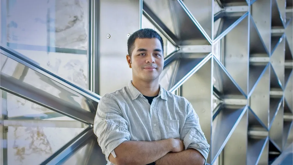
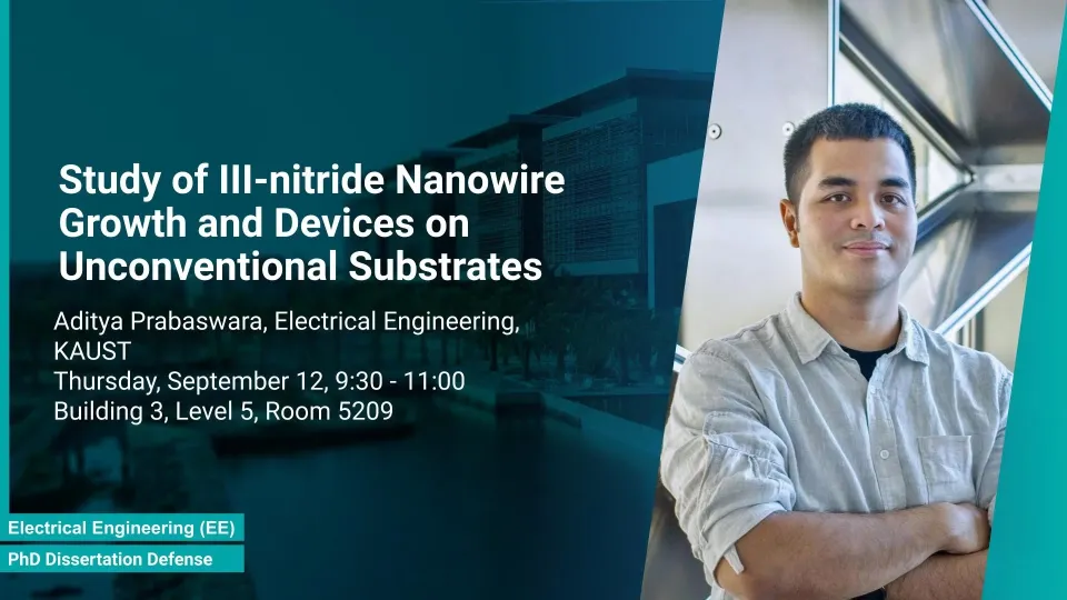
About Aditya Prabaswara Aditya Prabaswara Ph.D., Electrical and Computer Engineering III-nitride nanowires optoelectronic device fabrication molecular beam epitaxy Aditya Prabaswara received his bachelor's degree in Telecommunication Engineering from Institut Teknologi Bandung, Indonesia in 2011 and his Master’s degree in Electrical Engineering from Korea Advanced Institute of Science and Technology, South Korea in 2014. He joined Prof. Boon Ooi’s group in 2014 under KAUST’s CEMSE department for his Ph.D. Currently, he is working as a Postdoctoral Fellow at Linköping University, Sweden. Research Interests Aditya's research interests included Photonics and Optoelectronics. His main research topic involves the growth, characterization, and device Events Presented Events Sep 8 - Sep 14, 2019 Study of III-nitride Nanowire Growth and Devices on Unconventional Substrates Aditya Prabaswara, Ph.D., Electrical and Computer Engineering Sep 12, 09:30 - 11:00 B3 L5 R5209 semiconductors III-nitride nanowires optoelectronics This thesis aims to investigate the microscopic characteristics of the nanowires and expand on the possibility of using transparent amorphous substrate for III-nitride nanowire devices. In this work, we performed material growth, characterization, and device fabrication of III-nitride nanowires grown using molecular beam epitaxy on unconventional substrates including silicon substrates and fused silica substrates. We also investigated the effect of various nucleation layers on the morphology and quality of the nanowires.
Study of III-nitride Nanowire Growth and Devices on Unconventional Substrates Aditya Prabaswara, Ph.D., Electrical and Computer Engineering Sep 12, 09:30 - 11:00 B3 L5 R5209 semiconductors III-nitride nanowires optoelectronics This thesis aims to investigate the microscopic characteristics of the nanowires and expand on the possibility of using transparent amorphous substrate for III-nitride nanowire devices. In this work, we performed material growth, characterization, and device fabrication of III-nitride nanowires grown using molecular beam epitaxy on unconventional substrates including silicon substrates and fused silica substrates. We also investigated the effect of various nucleation layers on the morphology and quality of the nanowires.
Engage ORCID ShareClipboard Related Content Articles 3 Events 1 Related Links Publication on KAUST Repository View list of Publications on ORCID LinkedIn profile Personal Website